Transmission Electron Microscopy

Transmission Electron Microscopy: Unveiling Microcosmos

Transmission Electron Microscopy (TEM) is a high-resolution imaging technique using electrons transmitted through a thin specimen. It provides detailed views of atomic structures, crystal defects, and nanomaterials, indispensable for materials science, biology, and nanotechnology research.

Transmission Electron Microscopy

Overview

The world of microscopy has opened doors to realms invisible to the naked eye, allowing scientists and researchers to explore the intricate details of the microcosmos. Transmission Electron Microscopy (TEM) stands as one of the most powerful tools in this arsenal, providing unprecedented insights into the nanoscale structure of materials. In this comprehensive guide by Academic Block, we will explore the principles, techniques, applications, and advancements in Transmission Electron Microscopy.

I. Basics of Transmission Electron Microscopy

Historical Evolution

Transmission Electron Microscopy has a rich history dating back to the early 20th century. In 1931, Ernst Ruska, along with Max Knoll, built the first Transmission Electron Microscope, revolutionizing our ability to observe structures at the atomic level. Since then, TEM has undergone significant advancements, shaping the landscape of materials science, biology, and various other disciplines.
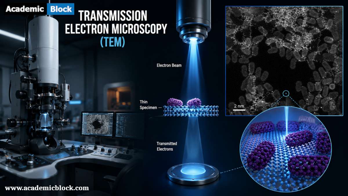
Operating Principles

Transmission Electron Microscopy operates on the principle of transmitting electrons through a thin specimen, allowing for high-resolution imaging. The core components of a TEM include an electron gun, condenser lenses, an objective lens, a specimen stage, and an imaging system. Understanding the interactions between electrons and matter is crucial to interpreting the resulting images.

Electron Sources

Electron guns are fundamental to TEM, providing a source of electrons for imaging. Two common types of electron sources are thermionic emission guns and field emission guns. Each has its advantages and limitations, influencing the resolution and performance of the microscope.

II. Techniques in Transmission Electron Microscopy

Sample Preparation: Achieving high-quality TEM images requires meticulous sample preparation. Specimens must be thin enough to allow electrons to pass through but thick enough to retain structural integrity. Techniques such as ultramicrotomy, ion milling, and cryo-electron microscopy are employed depending on the nature of the sample.

Contrast Mechanisms: Contrast in TEM images is generated through the interaction of electrons with different materials within the specimen. Techniques such as phase contrast, dark-field imaging, and Z-contrast enhance specific features, providing a wealth of information about the sample’s composition and structure.

Electron Diffraction: Electron diffraction is a powerful technique used in TEM to analyze the crystal structure of materials. By measuring the angles and intensities of diffracted electrons, researchers can determine the arrangement of atoms within a crystal lattice. This technique is vital for understanding the properties of various materials, including metals, minerals, and biological specimens.

III. Applications of Transmission Electron Microscopy

Material Science: TEM has played a pivotal role in advancing materials science by allowing scientists to study the microstructure of materials with unprecedented detail. From analyzing defects in semiconductors to characterizing nanomaterials, TEM has become indispensable in the development of new materials with enhanced properties.

Biology and Medicine: In the field of biology, TEM has been instrumental in unraveling the mysteries of cellular structures. Researchers use TEM to visualize organelles, cellular membranes, and even individual molecules. In medicine, TEM aids in understanding diseases at the cellular and molecular levels, contributing to the development of targeted therapies and diagnostic tools.

Nanotechnology: Nanotechnology relies heavily on TEM for imaging and characterizing nanoscale structures. Researchers use TEM to investigate nanoparticles, nanotubes, and other nanomaterials, providing insights into their properties and potential applications in fields such as electronics, catalysis, and drug delivery.

IV. Mathematical equations behind the Transmission Electron Microscopy

The mathematical principles behind Transmission Electron Microscopy (TEM) involve the interaction of electrons with matter and the subsequent formation of images. Several equations describe the behavior of electrons in a TEM system:

Schrödinger Equation: The motion of electrons is governed by the Schrödinger equation, which describes the wave function of a particle. In the context of TEM, this equation is used to understand the behavior of electrons as they pass through a specimen. The time-independent Schrödinger equation is given by:

H ψ = E ψ ;

Where:

  • H is the Hamiltonian operator.

  • ψ is the wave function of the electron.

  • E is the energy of the electron.

Electron Wave Equation: The de Broglie wavelength (λλ) of an electron is given by the de Broglie equation:

λ = h / p ;

Where:

  • h is Planck’s constant (6.626×10⁻³⁴ J⋅s).

  • p is the momentum of the electron.

The de Broglie wavelength is crucial in understanding the wave-particle duality of electrons and their behavior in the TEM.

Bragg’s Law: Bragg’s law describes the conditions for constructive interference of X-rays or electrons diffracted by a crystal lattice. In TEM, it is fundamental for understanding electron diffraction patterns. Bragg’s law is given by:

2d sin⁡θ = n λ ;

Where:

  • d is the lattice spacing.

  • θ is the angle of incidence.

  • n is an integer representing the order of diffraction.

  • λ is the wavelength of the incident electron beam.

Bragg’s law is essential for determining crystal structures and understanding the diffraction patterns observed in TEM.

Contrast Transfer Function (CTF): The Contrast Transfer Function is a mathematical description of how the contrast of an object is transferred to the image formed in the TEM. It is represented by the equation:

CTF = A(θ) ⋅ sin⁡ [ ϕ(θ) + CTFphase(θ) ] ;

Where:

  • A(θ) is the amplitude of the transfer function.

  • ϕ(θ) is the phase of the transfer function.

  • CTFphase(θ) is the phase reversal of the transfer function.

The CTF is crucial for understanding and correcting image contrast in TEM.

These equations represent fundamental aspects of the mathematical framework underlying the principles of Transmission Electron Microscopy. Understanding these equations is essential for researchers and scientists working in the field to interpret TEM results and optimize imaging conditions for various applications.

V. Advancements in Transmission Electron Microscopy

High-Resolution TEM: Recent advancements in electron optics and detector technologies have led to the development of high-resolution TEM, pushing the limits of imaging capabilities. These improvements enable researchers to visualize structures at the sub-angstrom level, opening new avenues for understanding nanoscale phenomena.

In-situ TEM: In-situ TEM allows researchers to observe dynamic processes occurring within a specimen in real-time. This technique is particularly valuable for studying phase transitions, chemical reactions, and mechanical properties at the nanoscale. In-situ TEM has broad applications in materials science, catalysis, and nanotechnology.

Cryo-TEM: Cryo-TEM involves imaging specimens at cryogenic temperatures, preserving their native structures and avoiding artifacts caused by conventional sample preparation methods. This technique is crucial for studying biological samples, macromolecular complexes, and soft materials, providing a more accurate representation of their structures.

VI. Challenges and Future Prospects

Sample Radiation Damage: One of the challenges in TEM is the potential damage to samples caused by the intense electron beam. Researchers are actively working on minimizing radiation damage through techniques such as low-dose imaging, adaptive focusing, and the use of advanced specimen support materials.

Integration with Other Techniques: The integration of TEM with other imaging and spectroscopy techniques, such as scanning electron microscopy (SEM), energy-dispersive X-ray spectroscopy (EDS), and electron energy loss spectroscopy (EELS), enhances the capabilities of TEM. This interdisciplinary approach provides a more comprehensive understanding of materials and biological specimens.

Artificial Intelligence in TEM: The integration of artificial intelligence (AI) and machine learning algorithms is poised to revolutionize TEM data analysis. These technologies can assist in image interpretation, automatic particle detection, and even guide experimental design, accelerating the pace of scientific discovery.

Final Words

In this article by Academic Block, we have seen that, the Transmission Electron Microscopy has evolved into a cornerstone technology, empowering scientists to explore the intricate world of nanoscale structures. From its humble beginnings in the early 20th century to the cutting-edge advancements of today, TEM continues to push the boundaries of what is possible in scientific research. As we stand on the brink of a new era in microscopy, the future promises even greater revelations, unlocking the secrets of the microcosmos and fueling innovations across diverse scientific disciplines. Please provide your comments below, thanks for reading!

This Article will answer your questions like:

+ What is Transmission Electron Microscopy (TEM) and how does it work? >

Transmission Electron Microscopy (TEM) is an imaging technique where a beam of electrons is transmitted through an ultra-thin specimen. The electrons interact with the specimen, and the transmitted electrons are used to form an image. The high resolution of TEM is due to the short wavelength of electrons, which allows for imaging at atomic scales.

+ How does TEM achieve high-resolution imaging of biological and material samples? >

TEM achieves high-resolution imaging through the use of electron beams with wavelengths much shorter than visible light. The interaction of electrons with the sample's atomic structure provides detailed information at the atomic level. Advanced electron optics and aberration correction techniques further enhance the resolution and contrast of TEM images.

+ What are the key principles behind electron beam interaction in TEM? >

In TEM, electrons interact with the sample through elastic and inelastic scattering. Elastic scattering provides information about the atomic structure and lattice parameters, while inelastic scattering provides data on the electronic structure and chemical composition. These interactions enable comprehensive analysis of the sample.

+ How does TEM compare to other electron microscopy techniques like SEM? >

While TEM provides detailed internal structure and atomic-level resolution, Scanning Electron Microscopy (SEM) offers detailed surface morphology and composition analysis. SEM uses scattered electrons to image surfaces, whereas TEM uses transmitted electrons for internal structure imaging, making TEM more suitable for atomic-scale studies.

+ What types of samples and materials are suitable for TEM? >

TEM is suitable for a wide range of samples including metals, semiconductors, polymers, biological specimens, and nanoparticles. Samples must be ultra-thin (typically less than 100 nm) to allow electron transmission. Advanced preparation techniques, like cryo-TEM, enable the study of sensitive biological materials.

+ How does TEM contribute to understanding atomic-scale structures and defects? >

TEM provides atomic-scale imaging, enabling the visualization of atomic arrangements and defects such as dislocations, vacancies, and interstitials. High-resolution TEM (HRTEM) and electron diffraction techniques reveal precise atomic positions and lattice structures, crucial for material science and nanotechnology research.

+ What role does electron optics play in TEM imaging? >

Electron optics in TEM involves electromagnetic lenses that focus and control the electron beam. Advanced electron optics, including aberration correctors, enhance image resolution and quality. Precise control over electron beam paths and interactions is critical for achieving high-resolution and contrast in TEM images.

+ What are the advantages of using TEM for studying nanoparticles and viruses? >

TEM offers unparalleled resolution and magnification, essential for studying the fine structural details of nanoparticles and viruses. It allows visualization of their morphology, size distribution, and internal structures at the atomic level, aiding in the development of nanotechnology and virology research.

+ How is contrast generated in TEM images? >

Contrast in TEM images is generated through electron scattering. Thicker or denser regions scatter more electrons, appearing darker, while thinner or less dense areas scatter fewer electrons, appearing lighter. Techniques like phase contrast and diffraction contrast further enhance image details.

+ What are the main components of a Transmission Electron Microscope? >

A Transmission Electron Microscope consists of an electron gun, electromagnetic lenses, sample holder, vacuum system, and imaging system. The electron gun generates the electron beam, lenses focus and direct the beam, and the imaging system captures the transmitted electrons to form high-resolution images.

+ What are the limitations and challenges of TEM technology? >

Limitations of TEM include the need for ultra-thin samples, complex sample preparation, and high operational costs. Challenges also involve maintaining high vacuum conditions, avoiding beam damage to samples, and interpreting complex data accurately. Technological advancements continue to address these issues.

+ How is data from TEM experiments processed and interpreted? >

Data from TEM experiments is processed using specialized software for image reconstruction, noise reduction, and quantitative analysis. Techniques like Fourier transform and digital filtering enhance image details. Interpretation involves correlating observed features with known atomic structures and materials properties.

+ What recent advancements have been made in Transmission Electron Microscopy? >

Recent advancements in TEM include the development of aberration-corrected electron optics, enabling sub-angstrom resolution. Innovations in cryo-TEM allow high-resolution imaging of biological specimens in their native state. Additionally, advances in direct electron detectors have improved image quality and data acquisition speed.

Hardware and software required for Transmission Electron Microscopy

Hardware:

  1. Electron Gun: The electron gun generates a focused beam of electrons, typically using either thermionic emission or field emission. It is a crucial component for the illumination of the specimen.
  2. Lenses and Apertures:
    • Condenser Lenses: These lenses focus the electron beam onto the specimen, ensuring a well-defined and focused illumination.
    • Objective Lens: The objective lens is responsible for magnifying the transmitted electrons and forming the primary image of the specimen.
  3. Specimen Stage: The specimen stage holds the sample in place and allows for precise positioning. It is often equipped with tilt and rotation capabilities for obtaining different views of the specimen.
  4. Electron Detector System: Various detectors, such as scintillators or solid-state detectors, capture the electrons transmitted through the specimen. Different detectors can be used for imaging or diffraction purposes.
  5. Vacuum System: TEM operates in a high-vacuum environment to minimize electron scattering and maintain a clear path for the electron beam.
  6. Camera System: Modern TEMs are equipped with high-resolution digital cameras for capturing electron images. These cameras are essential for converting the electron signal into digital images.
  7. Cryogenic System (Optional): For cryo-TEM, a cryogenic system is used to maintain the specimen at low temperatures, preserving biological samples in a near-native state.
  8. Computing System: A powerful computing system is necessary for data acquisition, processing, and analysis.

Software:

  1. TEM Control Software: This software controls the operation of the TEM, allowing users to adjust parameters such as beam intensity, focus, and imaging modes.
  2. Imaging Software: Software for acquiring, storing, and viewing digital images obtained from the TEM. It may include features for adjusting contrast, brightness, and performing basic image processing.
  3. Analysis Software:
    • Image Analysis Software: Specialized software for quantifying and analyzing TEM images. It may include tools for particle counting, measuring distances, and other morphological analyses.
    • Crystallography Software: For analyzing electron diffraction patterns and determining crystal structures.
  4. 3D Reconstruction Software (Optional): For tomographic studies, software for reconstructing three-dimensional structures from a series of 2D images obtained at different tilt angles.
  5. Simulation Software (Optional): Software for simulating TEM images or diffraction patterns to aid in the interpretation of experimental results.
  6. Database and Storage Software: Systems for organizing, storing, and retrieving large volumes of TEM data efficiently.

Key Discoveries where Transmission Electron Microscopy is used

DNA Structure: James Watson and Francis Crick’s discovery of the double-helix structure of DNA in 1953 was supported by X-ray diffraction data, including images obtained using TEM. Rosalind Franklin’s work with Maurice Wilkins, using TEM to capture images of DNA fibers, provided crucial insights into DNA’s structural features.

Virus Structure: In the 1950s and 1960s, TEM was pivotal in revealing the structure of viruses. The first images of the tobacco mosaic virus and other viruses provided essential information about their size, shape, and symmetry.

Cell Ultrastructure: Christian de Duve’s groundbreaking work using TEM in the 1950s led to the discovery of cellular organelles such as lysosomes and peroxisomes. TEM allowed researchers to visualize the internal structures of cells, advancing our understanding of cell biology.

Nanomaterials and Nanoparticles: TEM has been crucial in characterizing and understanding the properties of nanomaterials. Discoveries in nanotechnology, including the visualization of quantum dots, nanotubes, and other nanoscale structures, have relied heavily on TEM.

Discovery of Ribosomes: Albert Claude, Christian de Duve, and George Palade used TEM in the 1950s to discover and characterize ribosomes, the cellular structures responsible for protein synthesis. This work laid the foundation for our understanding of cellular processes.

Materials Science Advancements: TEM has been integral in materials science, contributing to the discovery and characterization of novel materials. For example, the observation of defects in crystalline structures and the analysis of nanoscale materials have led to advancements in semiconductor technology and materials engineering.

Neuroscience and Synaptic Transmission: TEM has played a crucial role in neuroscience, allowing researchers to study the ultrastructure of neurons and synapses. This has led to key insights into synaptic transmission and the understanding of various neurological disorders.

Discovery of Fullerenes: In 1985, Harry Kroto, Robert Curl, and Richard Smalley discovered fullerenes, a new form of carbon allotropes, which include the well-known C60 buckyball. TEM played a crucial role in characterizing the structure of these unique carbon molecules.

Catalysis and Nanocatalysts: TEM has been instrumental in studying catalysts at the nanoscale, enabling the design and optimization of nanocatalysts for various chemical processes. This has implications for catalysis in industrial applications and environmental science.

Advancements in Nanomedicine: TEM has contributed to the field of nanomedicine by allowing researchers to visualize and study nanoscale drug delivery systems, nanoparticles for medical imaging, and interactions between nanomaterials and biological systems.

Father of Transmission Electron Microscopy

The title of “father of Transmission Electron Microscopy” is often attributed to Ernst Ruska. Along with Max Knoll, Ernst Ruska constructed the first Transmission Electron Microscope (TEM) in 1931, which marked a significant breakthrough in the field of microscopy. This invention revolutionized scientists’ ability to observe structures at the atomic and molecular levels, providing a powerful tool for research in various scientific disciplines. Ernst Ruska’s pioneering work laid the foundation for the development and widespread use of Transmission Electron Microscopy in the decades that followed.

Facts on Transmission Electron Microscopy

Invention and Pioneers: Transmission Electron Microscopy was invented by German scientists Ernst Ruska and Max Knoll in 1931. Ernst Ruska later received the Nobel Prize in Physics in 1986 for his contributions to the development of the electron microscope.

Wavelength of Electrons: Electrons used in TEM have much shorter wavelengths than visible light. This allows TEM to achieve much higher resolution compared to optical microscopes, enabling the visualization of structures at the atomic and molecular levels.

Magnification Power: TEMs are capable of achieving magnifications in the range of millions, allowing researchers to observe structures with incredible detail. This high magnification is essential for studying nanoscale materials and biological specimens.

Sample Preparation Challenges: Sample preparation for TEM is a meticulous process. Specimens need to be very thin (typically less than 100 nanometers) to allow electrons to pass through, and various techniques, such as ultramicrotomy or ion milling, are employed.

Cryo-TEM: Cryo-TEM involves imaging specimens at extremely low temperatures, often below -150 degrees Celsius. This technique preserves the natural state of biological samples, reducing the impact of artifacts introduced by conventional sample preparation methods.

Electron Diffraction: TEM can be used for electron diffraction studies, providing information about the crystal structure of materials. Bragg’s Law is applied to interpret diffraction patterns obtained using TEM.

In-situ TEM: In-situ TEM allows researchers to observe dynamic processes occurring within a specimen in real-time. This capability is crucial for studying reactions, phase transitions, and mechanical properties at the nanoscale.

Contrast Mechanisms: Contrast in TEM images is achieved through different mechanisms, including amplitude contrast and phase contrast. Various staining techniques are often employed to enhance contrast in biological specimens.

3D Reconstruction: TEM can be used for tomographic studies, where a series of 2D images obtained at different tilt angles are reconstructed to create a three-dimensional representation of the specimen.

Electron Lenses: TEM uses electromagnetic lenses, including condenser lenses and objective lenses, to focus and control the electron beam. These lenses are crucial for achieving high-resolution imaging.

Environmental TEM: Some advanced TEM systems allow imaging in controlled environments, such as in the presence of gases or liquids. This capability expands the range of materials and processes that can be studied.

Quantitative Analysis: TEM is not only a qualitative imaging tool but also allows for quantitative analysis. Techniques such as energy-dispersive X-ray spectroscopy (EDS) and electron energy loss spectroscopy (EELS) provide information on elemental composition and electronic properties.

High Vacuum Operation: TEMs operate in a high-vacuum environment to minimize electron scattering and maintain a clear path for the electron beam.

Interdisciplinary Applications: TEM is widely used across various scientific disciplines, including materials science, biology, chemistry, physics, and nanotechnology, showcasing its versatility and importance in advancing research.

Academic References on Transmission Electron Microscopy

Books:

  1. Chapman, K. W. (2013). Practical Electron Microscopy: A Beginner’s Illustrated Guide. Springer.
  2. Egerton, R. F. (2005). Physical Principles of Electron Microscopy: An Introduction to TEM, SEM, and AEM. Springer.
  3. Goldstein, J., Newbury, D. E., Echlin, P., Joy, D. C., Romig, A. D., Lyman, C. E., & Fiori, C. (2003). Scanning Electron Microscopy and X-ray Microanalysis. Springer.
  4. Reimer, L., & Kohl, H. (2008). Transmission Electron Microscopy: Physics of Image Formation. Springer.
  5. Spence, J. C. H. (2013). High-Resolution Electron Microscopy. Oxford University Press.
  6. Hren, J. J., Carpenter, P. G., & Desjardins, A. E. (2010). Basic Electro-Optics for Electrical Engineers. SPIE Press.
  7. Cowley, J. M., & Moodie, A. F. (1957). The Scattering of Electromagnetic Waves from Rough Surfaces. Oxford University Press.
  8. Knoll, M., & Ruska, E. (1932). The Electron Microscope. Zeitschrift für Physik, 78(9-10), 318-339.

Journal Articles:

  1. Crewe, A. V., & Wall, J. (1970). Electron Microscopy of Radiation-Sensitive Specimens: Observation of Biological Molecules in Aqueous Solutions. Science, 168(3933), 1338-1340.
  2. Henderson, R., & Unwin, P. N. (1975). Three-dimensional model of purple membrane obtained by electron microscopy. Nature, 257(5521), 28-32.
  3. De Rosier, D. J., & Klug, A. (1968). Reconstruction of three-dimensional structures from electron micrographs. Nature, 217(5124), 130-134.
  4. Baker, T. S., & Cheng, R. H. (2012). A model-based approach for determining orientations of biological macromolecules imaged by cryo-electron microscopy. Journal of Structural Biology, 180(3), 386-396.
  5. Midgley, P. A., & Weyland, M. (2003). 3D electron microscopy in the physical sciences: the development of Z-contrast and EFTEM tomography. Ultramicroscopy, 96(3-4), 413-431.
  6. Egerton, R. F., Li, P., & Malac, M. (2004). Radiation damage in the TEM and SEM. Micron, 35(6), 399-409.
0 0 votes
Article Rating
Subscribe
Notify of
guest
0 Comments
Oldest
Newest Most Voted
Inline Feedbacks
View all comments
0
Would love your thoughts, please comment.x
()
x